
Matching Network Design for Power Amplifiers
21-Aug-2018

21-Aug-2018
Application note | WIPL-D Microwave Pro | Updated: October 2026
This application note explains matching network design for power amplifiers, using a commercial RF power transistor for the 2.5–2.7 GHz band as an example.
Discrete microwave transistors usually come with I-V curves and small-signal S and noise parameters, which is enough for linear and low noise amplifier design in a linear circuit simulator. Strongly nonlinear circuits such as oscillators and frequency multipliers need nonlinear time-domain or harmonic balance simulation, and nonlinear device models require advanced characterization and parameter extraction.
Power amplifiers are strongly nonlinear, yet they are still designed using linear techniques. The reasons are demanding and conflicting requirements: maximum output power, power gain, power added efficiency (PAE), acceptable nonlinear distortion and memory effects, for signals with a given modulation, peak-to-average power ratio (PAPR) and envelope statistics. A power transistor is also typically designed for a single application, and its optimum operating conditions are determined experimentally, using a setup beyond the reach of a typical designer. Manufacturers therefore publish the optimum conditions, and sometimes a complete reference design with PCB layout and bill of materials.
A designer still has room to verify a recommended design before prototyping, to modify it, or to adapt it, for example to a different substrate. This application note shows how to do that reliably using WIPL-D Microwave.
Manufacturers supply the optimum impedances that must be presented to the transistor input and output for the specified performance. The example is a transistor for the 2.5–2.7 GHz band (WiMAX, WiBro, BWA and multicarrier OFDM applications) operating in Class AB or Class C. Zsource is the optimum impedance at the gate and Zload at the drain.
Table 1. Optimum source and load impedances supplied by a manufacturer for an RF power transistor
| f [MHz] | Zsource [Ω] | Zload [Ω] |
|---|---|---|
| 2500 | 4.059 − j2.284 | 3.380 − j0.543 |
| 2525 | 3.679 − j2.593 | 3.265 − j0.546 |
| 2550 | 3.006 − j2.574 | 3.077 − j0.449 |
| 2575 | 2.355 − j2.190 | 2.892 − j0.336 |
| 2600 | 2.075 − j1.657 | 2.727 − j0.182 |
| 2625 | 1.930 − j1.179 | 2.564 − j0.034 |
| 2650 | 1.973 − j0.771 | 2.435 + j0.140 |
| 2675 | 2.017 − j0.557 | 2.286 + j0.340 |
| 2700 | 2.024 − j0.379 | 2.227 + j0.538 |
The impedances are very low, so designing the matching networks is not trivial. The challenge is to transform the 50 Ω system impedance to the required optimum values at the transistor terminals. In WIPL-D Microwave the optimum impedances are introduced through a Touchstone Z-parameter data block and graphed on a Smith chart (Figure 1).
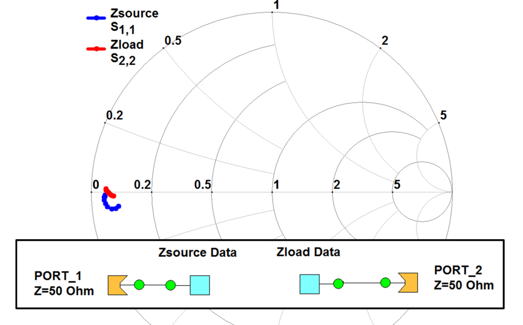
Figure 1: Optimum source and load impedances added as schematic entities through a Touchstone Z-parameter data block and graphed on a Smith chart in WIPL-D Microwave
There are many ways to match an impedance in a given band, using lumped elements, transmission lines or both. For amplifiers the topology must also provide DC paths for biasing, and it must decouple the terminating lines from DC bias currents and the bias terminals from RF currents.
DC blocking is typically a pair of parallel coupled lines that are a quarter wavelength long at the operating frequency, or a series capacitor. RF isolation of the bias terminal, which is important for amplifier stability, is usually a shunt short-circuited quarter-wave stub or a shunt inductor. At the operating frequency the stub represents an open circuit and does not load the matching network, and a properly dimensioned inductor must have sufficiently high impedance there.
In a power amplifier the harmonic content of the output signal matters. At the second harmonic an ideal short-circuited stub acts as a short circuit and blocks the signal from reaching the output. The impedance of an inductor is only twice that at the operating frequency, which may be insufficient. In addition, practical inductors with high inductance values have a low self-resonant frequency that can fall below the second harmonic, making their behavior there unpredictable.
The schematics recommended by the manufacturer (Figure 2) combine lumped and transmission line elements. Only the elements critical for high-frequency operation are considered.
Resistor R1 acts as a matching element together with a high-impedance quarter-wave bias line that is effectively short-circuited at its far end by capacitor C2. Capacitor C1 isolates the input port from DC currents.
Capacitor C1 prevents DC current from flowing through the output port. Biasing uses two shunt high-impedance lines, about a quarter wavelength long, short-circuited for the microwave signal by capacitors C2 and C3. The manufacturer recommends slightly different lengths for the two lines, which widens the bandwidth of second harmonic suppression. With equal lengths, sufficient suppression would occur only at a single frequency.
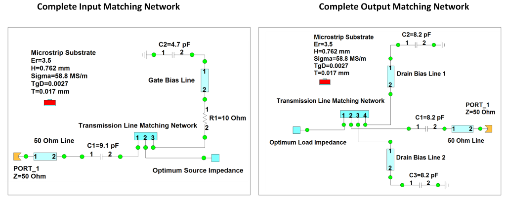
Figure 2: Schematics of input and output matching networks as suggested by the manufacturer in WIPL-D Microwave
Both networks include transmission line parts, implemented in WIPL-D Microwave as electromagnetic (EM) components (Figure 3).
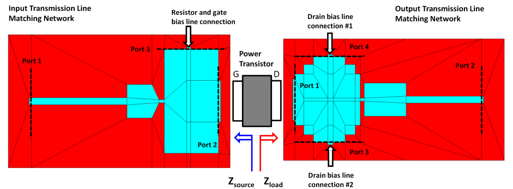
Figure 3: WIPL-D EM component models of the transmission line parts of the input and output matching networks
WIPL-D Microwave has built-in technology libraries with models of common transmission line discontinuities. The user can base the calculation on approximate analytic expressions or on full-wave EM simulation. The analytic expressions are accurate to within a few percent for mild discontinuities, but not when two, three, or four lines of drastically different widths are connected, as in Figure 3.
In these networks, the discontinuities are also physically very close, which means they are coupled. A circuit with coupled discontinuities cannot be modeled accurately as if they were uncoupled. Neither an analytic model nor an individual EM model of each discontinuity is adequate.
The long, uniform segments (terminating and bias lines) can be modeled efficiently with analytic components. The interface between the analytic and the EM part, and the connections between transmission lines and lumped elements, are modeled accurately by aligning the reference planes on the interconnecting ports and using de-embedding. Partitioning the circuit this way, within one design environment, makes WIPL-D Microwave a tool of choice for power amplifier design, and the built-in optimizer can then optimize all elements, including the EM components.
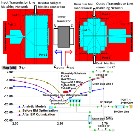
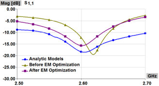 Figure 4: Simulated performance of the input matching network using the modeling and optimization options in WIPL-D Microwave
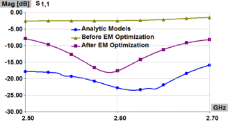 Figure 5: Simulated performance of the output matching network using the modeling and optimization options in WIPL-D Microwave
Accurate modeling of matching networks is crucial for successful power amplifier design. The set of simulation tools in WIPL-D Microwave provides a complete environment for accurate and efficient power amplifier design. The example of a commercially available power transistor explains the preferred matching network topologies and demonstrates the design flow. It also explains why electromagnetic analysis is necessary: otherwise, the effects of coupled discontinuities cause significant inaccuracy.
The design was carried out for the substrate recommended by the manufacturer. It can easily be adapted to another substrate, provided that the substrate thickness conforms with the height of the transistor lead and the first transmission line element remains wider than the lead.
How do I design a matching network for a microwave power amplifier? Start from the optimum source and load impedances supplied by the transistor manufacturer. Choose a topology that also provides DC biasing, DC blocking and second harmonic suppression. Model the network with analytic components where lines are uniform and EM components where discontinuities are coupled, then optimize the dimensions.
Why can’t each microstrip discontinuity be modeled separately? In power amplifier matching networks the discontinuities are physically close and therefore coupled. Their coupling adds effects that individual models miss, which is why the output network in this example showed only around 3 dB of return loss before optimization.
What impedances does a power transistor need? Very low ones. In the example, Zsource is 4.059 − j2.284 Ω and Zload is 3.380 − j0.543 Ω at 2500 MHz, which is why the first matching elements are wide, low-impedance microstrip lines.
Can the design be adapted to a different substrate? Yes, if the substrate thickness conforms with the height of the transistor lead and the first transmission line element remains wider than the lead.
Section: Microwave Circuits
Related application notes: Cavity Filter Design and Optimization | All application notes
Download the full application note MW_013 (PDF)