Differential Filter Design and Optimization

This note explains how to analyze and optimize a general differential microwave circuit using WIPL-D design environment. Weather it is the circuit or EM component the differential/common mode analysis can be carried out within WIPL-D Microwave Pro by adequate connection of several transformer elements to convert single-mode S parameters to differential/common mode S Parameters.

The innovative differential filter (taken from the literature) has been used to illustrate the analysis and optimization procedures. The filter has been analyzed as ideal transmission line circuit, as microstrip schematic and as 3D EM component. Converting ideal transmission line circuit into the realistic microstrip layout, causes several parasitic effects to occur, not included in the ideal model. The optimization process was applied to EM model since it includes all of the parasitic effects.

The modeling method demonstrated here can be applied to directly obtain differential/common mode S parameters of other differential components, such as amplifiers, couplers, antenna matching networks, etc.

View PDF

Rectangular Waveguide
Iris-Coupled Filter

In this application note, simulation of a band-pass, iris-coupled waveguide filter is described. The irises will be located on the both sides of the standard WR-90 waveguide. The iris-coupled filter was created from the scratch in WIPL-D Pro CAD. Two symmetry planes (Symmetry and Anti-Symmetry) have been applied to reduce the complexity of the simulations. Two Waveguide Ports were used as feeders.

The model of iris-coupled filter was simulated from 9 GHz to 12 GHz in 16 frequency points. To ensure high accuracy, the convergence of the results has been checked. After the convergence has been confirmed, dimensions of the filter were tuned to set values of S11 in the pass-band (10.19 GHz to 10.82 GHz) below -20 dB.

Computer used for these simulations is regular desktop or laptop, running the problem in couple of seconds per frequency point. Very low number of unknowns was used, resulting in usage of inexpensive hardware platform.

View PDF

Effective Antenna Design by
EM-Circuit Co-Simulation

The goal of a circuit-EM co-simulation is to alleviate the computational complexity decomposing the complete system into parts that need to be simulated using full-wave approach, and parts that would be modeled by predefined library components. The major benefit is that any antenna or antenna component of interest can be included and electromagnetically simulated, on-the-fly, at the circuit simulation runtime.

WIPL-D 3D EM solver and WIPL-D MW circuit solver present dynamically connected software. They are fast and accurate in co-simulation. In co-simulation, number of unknowns is dramatically reduced because of separating one big EM computational problem into many small problems.

Here, circuit is implemented in microstrip technology. It consists of two microstrip patch antennas and feeding network: microstrip lines, microstrip T junction and bends. System is analyzed in frequency band 9 GHz up to 11 GHz in 9 uniformly distributed points. Central operating frequency is 10 GHz. Simulation time is measured in seconds on any standard desktop or laptop.

View PDF

Bond Wires as Interconnect Technology

Accurate modeling of the bonding wires is essential to successfully utilize semiconductor bare dies and achieve a large scale of integration of modern microwave front ends. WIPL-D Microwave provides a complete design environment where electromagnetic and circuit simulation can be efficiently applied to examine the influence of interconnects to the performance of an integrated system.

The limitations of the single wire bonds regarding the relatively narrow return loss bandwidth have been illustrated through the analysis of performance degradation of an amplifier. The improvement of the characteristics when double wire bonds are utilized are presented and the mechanism of the improvement explained.

The selected examples concentrate on the applications in the frequency range around 24 GHz. As the operating frequency goes higher, the effects of interconnects become more severe and some means of compensation of bond wire connections described in the literature must be utilized to keep the return loss at reasonable values or a different interconnect technology, such as flip chip of micro ball grid array (µBGA), has to be considered.

View PDF

Dielectric Resonator Filter [Verified by Measurements]

The application note deals with complex dielectric resonator filters with numerous tuning elements. Careful comparison to measured results is carried out in each step. The story unfolds from a simple single cavity with the loop made of coax cable. The cubic dielectric puck is inserted at the middle to modify the resonance. In the next step, the puck is hollow, which changes the resonance again. WIPL-D sweeper is used to demonstrate how the resonance shifts by merely changing puck length. Such models are simple and the simulation is carried out in seconds in the entire frequency band. Single cavity with solid puck is the most important model. It is tuned to achieve a wide and deep resonance, which coincide with the measured results. A single cavity model is very fast and lasts only a couple of seconds per frequency point, where powerful built-in interpolation allows using only 11 frequency points.

In the last step, a single cavity is mirrored and connected to the second cavity with goal post. The simulation is still carried out in seconds per frequency point at regular desktop or laptop PC.

View PDF

3-Port Wilkinson at High Microwave Frequencies

The accurate modeling of the effects occurring at high microwave frequencies is the key to successful design of a Wilkinson power combiner/divider. WIPL-D Microwave provides a complete environment required for a design of these circuits including circuit and electromagnetic co-simulation.

Example of a design cycle has been provided. The cycle starts with the analysis of an ideal, by-the-book circuit schematic, continues to a more detailed schematic with models for microstrip discontinuities, and is then further expanded with the introduction of an EM component to model a complete microstrip circuit with high accuracy. Finally, the impact of a real-world resistor is demonstrated. The impact of each modeling step to degradation of circuit performance comparing to an ideal circuit is illustrated and explained in details. A designer is therefore provided with a clear understanding of what to expect and how to mitigate the potential problems at early stages of the design – it will be a good practice to utilize the smallest resistor size available, and, if possible, pick a substrate so that line-to-resistor-pad length ratio is maximized.

View PDF

Cavity Filter Design and Optimization
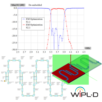
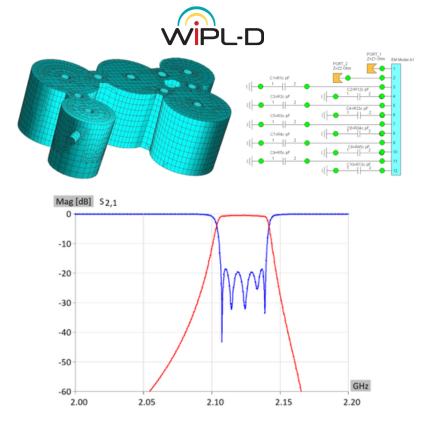
This application note describes efficient combination and interoperability of components of WIPL-D software environment (WIPL-D Pro CAD, WIPL-D Microwave Pro, WIPL-D Pro, WIPL-D Optimizer) for design, modeling, simulation and optimization of cavity filters. Rather complex model of a 2.1 GHz pass-band filter with 5 cavity resonators is imported, meshed, simulated (WIPL-D Pro CAD, WIPL-D Pro) and then quickly optimized invoking WIPL-D Optimizer from WIPL-D Microwave Pro, a linear circuit simulator.

The approach demonstrated in this application note assumes that the electromagnetic (EM) filter simulation is performed only once and the subsequent optimization is performed on a combined 3D/circuit model. The tuning schematic elements are in fact capacitors. The capacitance of the capacitors is tuned to emulate the inward and outward movement of the tuning screws. Such an optimization process is extremely fast and the tuning of the filter to the specified mask is very efficient.

WIPL-D suite has a variety of choices for modeling of cavity filters which can be customized according to the specific design. In that sense, WIPL-D Pro is used with simplified geometries, while WIPL-D Pro CAD is used for detailed models imported from popular CAD tools.

View PDF

Designing a Band Pass Filter with WIPL-D Filter Designer

A process of microstrip filter design has been described in this application note with a special focus on a technique of filter optimization, a simplified case of Space Mapping method. As a result of the design process a microstrip filter ready for sample fabrication is available with minimum human and numerical effort. The success of the design should be high as the limitations of a standard fabrication process are taken into account during the design. This includes the choice of the best suited substrate and the dimensional constrains.

There was no need to use any special piece of computer hardware as all of the simulations required were performed with high numerical efficiency on a standard desktop machine.

View PDF

WIPL-D Pro CAD Modelling Tutorial - Cavity Resonator Filters

The aim of this application note is to focus to modeling cavity filters in WIPL-D Pro CAD in a form of step by step document. The six cavities filters are based on relatively simple cylindrical cavities, each of the having tuning screws. Separate tuning screws are used for tuning the coupling between cavities.

The document first explains basic concepts, modelling via built-in primitives such as cylinder or cuboid. The building blocks are transformed and positioned via rotate/translate/multiple copy. More complex objects are made via sweep. The building blocks are assembled by using various Boolean operations, such as unite, subtract, imprint, unite simplify. The entire model is made fully parametrized so that it can be tuned/optimized. The document also explains the basic principles of WIPL-D pro CAD and offers tips for modifying projects via external applications, such as Notep/MatLab. The final step is adding the WIPL-D Pro CAD built-in ports to make a simulation ready project.

View PDF

High Level Miniaturization for Quadrature Hybrid Directional Coupler

This application note demonstrates how compact quadrilateral (branch-line) hybrid directional couplers can be designed efficiently using the WIPL-D Pro CAD. The designs are simulated by using the traditionally fast WIPL-D full wave 3D EM simulation.

The CAD tool enables easy and fast modeling of arbitrary structures using numerous built-in primitives and manipulations. In-house code for automatic meshing into quadrilateral patches, especially optimized for WIPL-D HOBF kernel, is employed.

The WIPL-D kernel enables fast and accurate simulation of PCB structures on inexpensive machines. The traditional coupler realized in microstrip technology is simulated in just a couple of seconds per frequency. As a result of a miniaturization, its size was almost halved. However, the miniaturization requires a careful design of artificial transmission lines with numerous fine details. EM simulation of such a device is much more demanding as it requires a large number of unknowns, but the high efficiency of the simulations is preserved as it takes only a couple of minutes per frequency point.

All the details significant for EM simulation such as losses, finite metallization thickness, finite size of the substrate and the ground conductor, location of the feeding point etc. are included in the model. The results presented include return loss at all of the ports, power division between the output ports, isolation between the input ports and finally the phases of the signals at the two output ports.

View PDF

Divider in Substrate Integrated Waveguide Technology

This application presents capabilities of WIPL-D software suite for full wave electromagnetic simulation of waveguide divider realized in substrate integrated waveguide technology, along with simulation results and requirements. WIPL-D is modern and extremely efficient Method of Moments full wave 3D EM simulator.

The divider in wave guide technology is moderate size model with certain smaller details, so WIPL-D advantages are pronounced in full extent. The simulation model has low number of mesh elements and low number of unknown coefficients needed to determine current distributions. The code executes rather quickly on inexpensive CPU platforms thanks to excellent parallelization capabilities. The simulation model of the waveguide divider originates from the provided CAD file, imported into WIPL-D Pro CAD. The model is symmetrical so only quarter of the model is simulated. This dramatically saves resources and simulation time. The device is designed for 60 GHz.

The simulation is carried out by using only CPU technology considering the fact that the model is not electrically large. The simulation requires only 8,100 unknown coefficients in MoM matrix, but it is carried out 4 times to generate results for all 5 ports (model symmetry). The total simulation time per frequency point is 39 sec on multicore desktop PC:

View PDF

Round Rod Interdigital Filter Optimization Using WIPL-D

This application note presents the results of round rode interdigital filters optimization using WIPL-D Pro, a full wave 3D electromagnetic simulation software empowered with Optimizer, a WIPL-D add-on tool.

Two filter responses have been considered, one with 180 MHz bandwidth and the other with 240 MHz bandwidth, both centered around 3.75 GHz. The lengths of the resonators, the gaps between the resonators and the height of the metallic box have been optimized using WIPL-D Optimizer. The optimization iteration takes only under 30 sec on any modern quad core laptop or desktop computer.

The illustrative examples of 5th order round rod interdigital filter optimization has been presented. The examples demonstrate that WIPL-D Pro can be successfully used to aid the real life design of a important filter structure. The basic strengths of the full 3D EM simulation program are high accuracy and extremely fast simulation which allows for quick optimization against various filter specifications.

View PDF