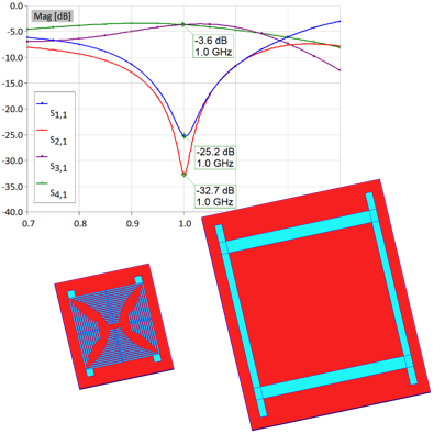
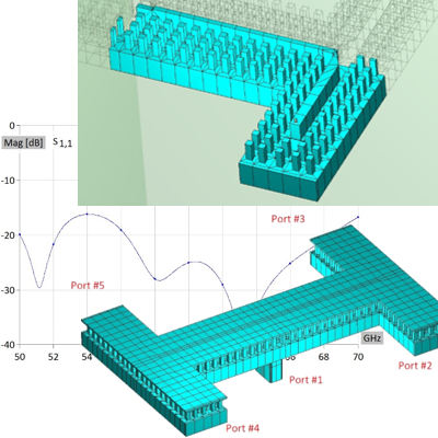
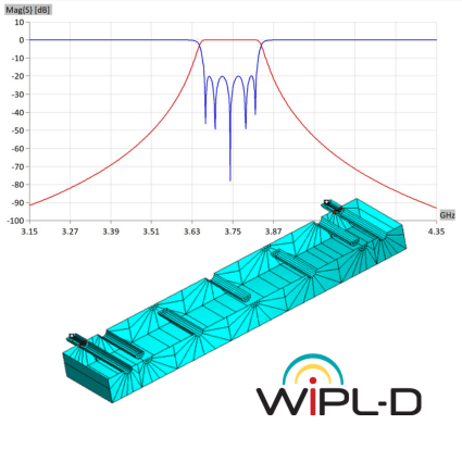
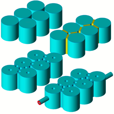
Linear Transistor Modeling Using Equivalent Circuits

The accurate transistor characterization is a starting point to carry out an amplifier design. Lumped circuit equivalent transistor models are compact and versatile means of providing reliable S parameter data. WIPL-D Microwave provides a complete environment to implement these models.

The modeling of a commercially available low power packaged GaAs HEMT has been illustrated. The partitioning of the transistor equivalent circuit to intrinsic and extrinsic elements has been presented and physical grounds behind each of the elements explained in brief. It has been shown that S parameters calculated using the model are highly accurate and can be utilized to overcome the limitation imposed with sparsely tabulated transistor data, e.g. to find the optimal biasing point for a desired application.

WIPL-D Microwave design environment provides required flexibility to implement a schematic of any commonly used linear transistor model.

View PDF

Rectangular Waveguide Interdigital Filter

This application note describes simulation of a band-pass, interdigital filter in rectangular waveguide technology. The filter was modeled using WIPL-D Pro CAD by using native editor and built-in primitives.

Symmetry plane has been utilized to reduce the complexity of the structure and two Waveguide Ports were used as feeders. The model was simulated from 5 GHz to 14 GHz in 26 frequency points. To ensure high accuracy, the convergence of the results has been checked. After the convergence study, dimensions of the filter were tuned to set values of s11 in the pass-band (8.30 GHz to 10.86 GHz) below -20 dB.

Computer used can be any desktop or laptop, desirably with higher number of CPU cores, with simulation time per frequency measured in
seconds.

View PDF

Matching Network Design for Power Amplifiers

The adequate modeling of matching networks is crucial for the success of power amplifier design. Due to a set of simulation tools included, WIPL-D Microwave provides a complete environment for accurate and efficient modeling and design of power amplifiers.

Example of a commercially available power transistor has been presented to explain the matching network topologies preferred for the power amplifier application and to demonstrate the outline of the complete design flow. The necessity to introduce electromagnetic analysis to accurately model typical power amplifier matching networks or otherwise face the significant inaccuracy due to the effects of coupled discontinuities has also been explained.

The design has been carried out for the microstrip substrate recommended by a manufacturer. If necessary, it can be easily adapted to any other substrate preferred providing that the substrate thickness conforms with the height of the transistor lead and the first transmission line element in the networks remains wider than the width of the transistor lead.

View PDF

Power Detector with Zero-Bias Schottky Diode

The design of a power detector can be easily accomplished if the right set of tools is available. WIPL-D Microwave is a one stop design environment providing a microwave circuit designer with several modeling options. The modeling using analytical elements can be smoothly expanded to EM analysis as an automated transfer of any schematic comprising elements with adequate layout representation to a 3D EM component is available whenever more accurate modeling is
required.

A choice between non-matched or matched power detectors is driven by the context of a particular application. For the case of a matched detector, the simplest matching network topology is preferred where detector sensitivity is a must. However, the return loss values obtained by a simple network may not be sufficient for some applications. If this is the case, a more complex matching network must be designed trading-off the sensitivity for favorable return loss values. To accurately account for all the effects occurring within the matching network, use of electromagnetic modeling is highly recommended.

View PDF

Multi-hole Waveguide Coupler

Multi-hole waveguide coupler is extension of single-hole coupler, designed to increase the operational bandwidth. The performance is based on size of the coupling holes and distance between them, since it is important to achieve wave amplification in the through-direction and cancellation in the opposite direction.

The waveguides used correspond to standard X-band WR-90, with dimensions of 22.86 mm by 10.16 mm. The waveguides are coupled through a series of rectangular cross-section holes arranged in a zig-zag order.

Simulation is performed at low number of frequency points due to powerful built-in interpolation. The hardware requirements are minimum, any standard desktop or laptop yields simulation time measured in seconds, owing to rather small number of unknowns.

View PDF

7-Port Divider

In this application, we simulate 7-port divider from 1.4 GHz to 1.6 GHz. This device is realized in microstrip technology, fed by probe with SMA connector at Tx port and the remaining 6 ports (Rx) are microstrip ports.

The model was made by using WIPL-D Pro as parametrized geometry (defining symbols, nodes, creating plates…). It is very simple process, but it takes a bit more time than the other possibilities (import of the DXF or any other geometry file, building the model in WIPL-D Pro CAD). The result is optimal mesh with minimum simulation time. The process is done more efficiently if the Copy/Layer manipulation is used.

A low number of frequency points is possible owing to built-in interpolation. In WIPL-D pro, even a 7-port divider is considered as electrically small structure. The number of unknowns and simulation time are minimum, so the simulation was carried out on regular desktop in just a couple of seconds.

View PDF

SPDT Shunt PIN Diode Switch

Design of various microwave circuits using semiconductor devices can be carried out utilizing WIPL-D Microwave. Many types of diodes, such as PIN and Schottky diodes, or transistors operating in a linear regime, can be simulated by inserting into a schematic a suitable equivalent circuit usually provided by a manufacturer. Other schematic elements from the libraries available, including ideal, microstrip, co-planar or coaxial elements, can be subsequently added to the schematic to complete the design of complex microwave circuits such as switches, detectors, amplifiers, oscillators etc.

The application note illustrates the PIN diode through the design of single pole double throw (SPDT) switch utilizing two PIN diodes. The diodes are represented in a form of an equivalent circuit.  Due to the operating principle of the switch, both ON and OFF equivalent circuits are used in the same circuit.

An illustrative example of a SPDT PIN diode switch simulation using WIPL-D Microwave demonstrates that besides main strengths in EM related problems, the WIPL-D suite provides a complete environment for design of complex microwave circuits including those using semiconductor devices.

View PDF

Lowpass Filter Design

Three models of filter will be designed and analyzed using WIPL-D powerful built in feature Filter Designer. Filter Designer is user-friendly, wizard-like GUI with straightforward two-stage filter. It is intended for automated design of lowpass, highpass, bandpass and bandstop filters of Chebyshev and Butterworth type.

Here, the filter type is lowpass and approximation is considered to be Chebyshev. The first model is implemented as LC ladder, the second one as transmission line while the third is microstrip filter. The third model is also simulated in WIPL-D 3D EM solver by using full electromagnetic analysis.

Operating band of interest is between 0.014 GHz and 2.8 GHz. Due to powerful built-in interpolation, it is sufficient to run the model in 11 frequency points (EM simulation) at any standard desktop or laptop. Simulation time for circuit models is negligible, while for full-wave EM model is a couple of seconds per frequency point.

View PDF

Metallic Cover over Wilkinson Power Divider

The Wilkinson power divider is a rather simple microwave circuit that allows equal splitting the input power to two of the identical output ports. The EM simulation carried out in the WIPL-D Pro 3D EM solver is itself simple, regardless the high operating frequency of 25 GHz and extremely thin substrate (0.005 mm with Er=3).

The application note demonstrates the most efficient way to model microstrip ports using two trapezoidal plates with a short/thin wire in between. Both wire ends are connected to metallic quads via triple junctions, which instructs the kernel to consider all three nodes to be in electrical connection. Such feeding mechanism inherently enables very low reflection loss. The lumped resistor is realized via concentrated loading.

A metallic box is added to the model of the divider to decrease EM coupling with neighboring devices. The performance of the divider with and without the box is compared. The results are as expected: very low return loss for microstrip ports, equal power division (-3 dB) between the input and the outputs, very good isolation between the output ports and rather low influence of adding the metallic cover.

View PDF

Design Flow for Microstrip Bandpass Filter

The accurate and efficient design of a microstrip bandpass filter can be easily accomplished by using WIPL-D design suite. It integrates microwave circuit, EM, radiation and near-field analysis within a single design environment.

The built-in tool Filter Designer allows direct synthesis of a microstrip filter circuit based on the user specification through user-friendly, wizard-like interface. The filter comprising analytic microstrip elements can be optimized to meet the specifications and then smoothly transferred to the EM model. A metallic box can be added to enclose the filter and study the effects of the shielding to the filter performance. The effects occurring in the box can alter the performance related to fundamental and especially to parasitic bandwidths. The effectiveness of techniques to suppress the box modes can be tested by full wave EM simulator immediately at simulation stage without expensive and time consuming rework once filter samples have been made.

View PDF

Microstrip Combline Bandpass Filter

A successful simulation of microstrip combline bandpass filter is demonstrated in this application note. The software tool used for the simulation is WIPL-D Pro software, a full wave 3D EM Method-of-Moments (MoM) based solver.

Simulation of one of the classical printed structure, the microstrip combline bandpass filter, was performed in a reasonable time on cost-effective, moderate computer platform. The fabrication of the microstrip filter prototype can follow immediately after the optimization.  The optimal dimensions of the filter resonators, input and output lines and the gaps between the lines are all realizable in any standard microstrip technology. In addition, dielectric parameters have been chosen targeting a popular, commercial substrate.

The combline filter was simulated between 4.0 GHz and 5.5 GHz. The efficient Fitter, which is part of the WIPL-Graph window, enabled the wideband response of this microstrip filter to be accurately interpolated from model simulation at 37 discrete frequency points.

Described bandpass filter is very simple, but it still has very good properties as calculated S-parameters confirm the existence of a transmission zero above the passband which can be used to increase the selectivity at high passband edge.

According to all of the analysis details presented, it can be concluded that WIPL-D software is very suitable for the simulation of various microstrip filter structures for both, commercial and academic purposes.

In addition, the practical and educative value of this document should be recognized. This document with published dimensions of the structure can be used as a starting point for microstrip combline bandpass filter design and further research.

View PDF

Microwave Circuits Design in WIPL-D Microwave

Simulation of complex microwave circuits presents a challenge for modern computational software. Using circuit level analysis is recommended option for the starting calculations in order to get results quickly. In circuit solvers, all circuit elements are modeled by predefined library components whose calculations are performed faster than calculations in full-wave EM analysis, even over a wide frequency range, practically on-the-fly.

WIPL-D Microwave is fast, accurate and easy-to-use software tool, what is proofed by several simulation examples. WIPL-D Microwave is compatible with many other software tools because of supported Touchstone file import. It is integrated with WIPL-D EM solver, WIPL-D Optimizer and WIPL-D Time Domain Solver.

The examples of circuit designs include single-stub tuner with rectangular waveguides (matched at 10 GHz), Diplexer operating at 2 GHz and 2.2 GHz, and Chebyshev impedance transformer in coaxial technology from 2 GHz up to 8.5 GHz. Computer required for these simulations is any standard desktop or laptop PC.

View PDF