
Power Detector with Zero-Bias Schottky Diode
24-May-2014

24-May-2014
Application note | WIPL-D Microwave Pro | Updated: November 2026
This application note describes the design of a zero-bias Schottky diode detector for microwave power detection, using the WIPL-D Microwave design environment. It covers non-matched and matched detector circuits, matching networks and EM modeling.
A power detector is an important part of many microwave systems. For example, it is frequently used in transmitter systems to monitor the power coming out of a power amplifier. If it is connected in a loop with a variable attenuator and a control logic circuit, the power of the amplifier can be adjusted to a required level.
At the receiver side, a power detector can be used in several ways. In channelized receivers, comprising a battery of narrowband filters, a power detector can be placed at each filter output, which allows instantaneous monitoring of the spectrum with a resolution of a filter cell in the frequency span of the battery. Along with the increased interest in simplifying transceivers, power detectors have re-emerged. The most promising solution, the so-called six-port topology, uses power detectors at the receiver side to replace the classical method of down-converting the signal to baseband using a mixer.
The simplest way to design a detector is to use a zero-bias diode, place it on the 50 Ω transmission line, and provide adequate paths and short circuits for DC and RF currents. A zero-bias diode does not require any external bias to operate as a detector, and for a number of applications a non-matched design is adequate. The example is a non-matched detector for a center frequency of 24 GHz and a span of 250 MHz, on a dielectric substrate with a relative dielectric constant εr = 3.5 and a thickness h = 0.254 mm.
The schematic in Figure 1 models the diode with lumped elements. Resistor Rs = 10.3 Ω models the series diode resistance, and capacitance Cj = 0.13 pF arises from the diode junction. Resistance Rj models the junction resistance. For zero-bias diodes the junction resistance is very high and can be excluded from the schematic. However, many detector diodes are used with a bias, and then the influence of Rj must be considered. The diode is grounded on the cathode side for the microwave signal.
The microstrip elements are modeled with analytical models, and the schematic is very simple because no matching is required. A short taper interfaces the relatively narrow line, which connects the diode leads, to the terminal 50 Ω microstrip line. Between the taper and the circuit port, a shunt quarter-wavelength transmission line is connected, with both a radial stub and a short circuit to ground at its other end.
A radial stub is basically a wideband capacitance to the microstrip ground. It represents a short circuit for the microwave signal, which transforms into an open at the connection with the terminal line, so the terminal line is not loaded by the short. In parallel to this capacitive connection, a conductive connection to ground must allow the detected DC current to flow through the diode. It is conveniently made with a via (plated through hole). At microwave frequencies, however, the parasitic inductance of a via gives a relatively high reactance, and the via deviates significantly from a short circuit for the microwave signal, which is why it is paired with a radial stub.
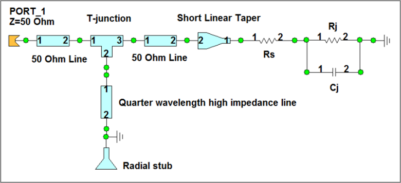
Figure 1: Schematic of the non-matched power detector using analytical microstrip elements from the WIPL-D Microwave library
The microstrip layout of the non-matched detector (Figure 2) was generated as an electromagnetic (EM) component directly from a schematic similar to Figure 1, with a single mouse click, using the schematic export to 3D EM model feature in WIPL-D Microwave. The only adjustment the user has to make is removing the schematic representation of Rs, Cj, Rj and the ideal connections to ground, because these elements have no adequate layout representation.
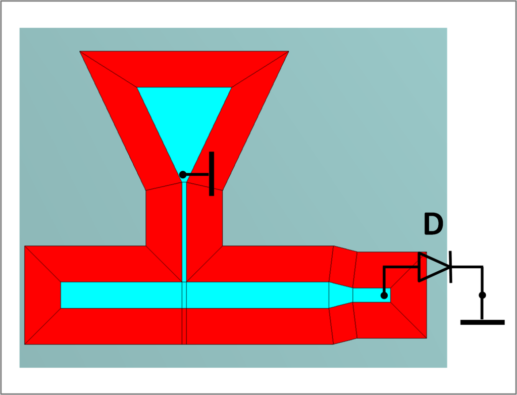
Figure 2: Microstrip layout of the non-matched power detector automatically generated from a circuit schematic
The layout in Figure 2 is for illustration only. For such a simple circuit, calculations with analytical microstrip models are sufficiently accurate, so an EM component is not necessary. The calculated return loss of the non-matched detector (Figure 3) is approximately 2 dB in the 22–26 GHz band.
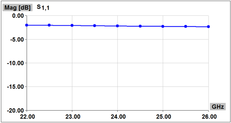
Figure 3: S parameters of the schematic from Figure 1
When a detector with such a poor match is used in a transmitter power control loop, it is preceded by a directional coupler with a typical coupling coefficient of −20 dB or less. Because of the loose coupling, the poor match of a non-matched detector does not affect the performance of the amplifier or of the transmitter chain as a whole.
In applications where a detector is used after a filter or connected at the ports of a six-port receiver, a poor match has a significant effect, because the performance of these circuits is very sensitive to the impedance presented at their terminals. For such applications a good match of the power detector is essential. The location of the diode reflection coefficient in the Smith chart is shown in Figure 4.
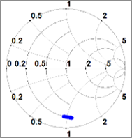
Figure 4: Diode reflection coefficient
A simple matching network should be used to match the diode, otherwise the insertion loss introduced by the network may affect the sensitivity of the detector. An example of such a network, comprising only two lumped elements, is shown in Figure 5. The schematic also contains a transmission line that models the diode pad effect, which is not negligible at the frequency of interest. The recommended pad size is indicated in the figure.
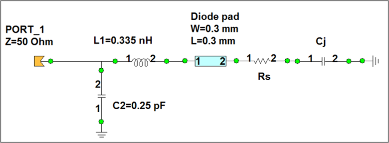
Figure 5: Lumped element matching circuit
The simulated return loss with optimized lumped element values is shown in Figure 6. The return loss is significantly improved compared with the non-matched case, reaching a maximum of approximately 15 dB at 24 GHz.
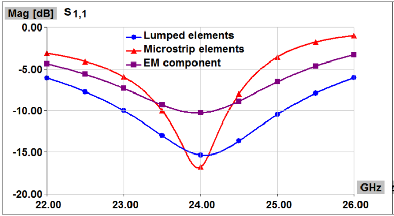
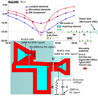
Figure 6: Comparison of simulated S parameters for the detector schematics from Figures 5, 7 and 9
Matching with lumped elements is not adequate at such a high frequency of operation. A network of distributed elements should be used instead. One possible solution is to replace the L-C matching section from Figure 5 with a series and a shunt transmission line, as shown in Figure 7, a complete microstrip schematic of the matched detector.
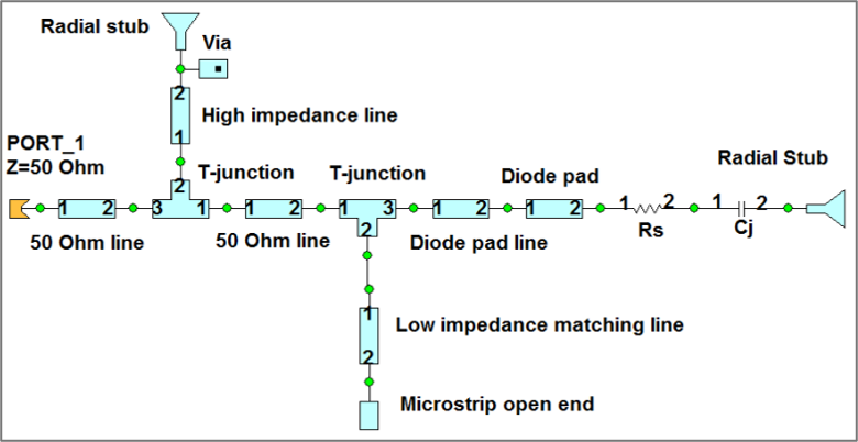
Figure 7: Microstrip element matching circuit
The simulation results for the schematic from Figure 7 are shown in Figure 6. Around 24 GHz the return loss is better than 15 dB. However, the return loss curve is very steep around the minimum. This indicates that an error in circuit dimensions during fabrication, or a variation of the diode equivalent circuit parameters from one sample to another, may shift the minimum to another frequency.
The analytical element that models a microstrip T-junction is not accurate when lines of considerably different widths are connected, as with the 69 Ω line and the 20 Ω line here. EM modeling of the diode matching circuit is therefore highly recommended. In WIPL-D Microwave, generating a complete EM component for the layout of the whole matching network is straightforward, because the program automatically translates the analytical elements into an EM component (Figure 8). The figure shows the complete matched detector microstrip circuit and the locations of the short circuits at DC and at microwave frequencies. It also includes the layout of the radial stub at the diode cathode, which is not part of the designed matching network.
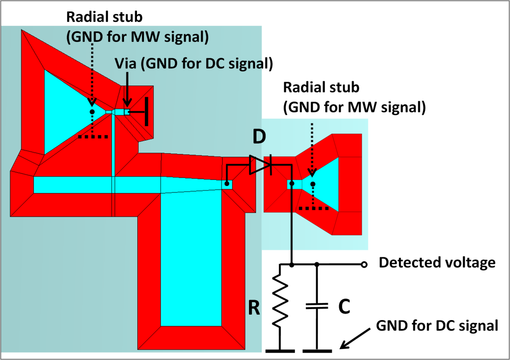
Figure 8: A complete layout of the matched detector
Resistor R and capacitor C are external components that must be added in a real detector circuit but are not relevant for high-frequency simulations. The resistance should be dimensioned to ensure efficient power transfer of the detected signal to an external circuit, and it is usually set equal to the video impedance of the diode (the impedance of the diode as a baseband signal source). The capacitance C is selected according to the required bandwidth of the detected signal and prevents noise outside the band from affecting detector sensitivity.
To finish the design, the EM component of the matching network is optimized with the other elements of the detector circuit connected. All elements are assembled in the schematic in Figure 9. The return loss of the optimized circuit (Figure 6) is in the range of 10 dB around the frequency of 24 GHz. The minimum is not as steep as in the schematic from Figure 7, which indicates lower sensitivity to fabrication tolerances and to the spread of diode characteristics. However, a value of 10 dB may not be sufficient for some applications, for example where a filter is connected to the detector input.
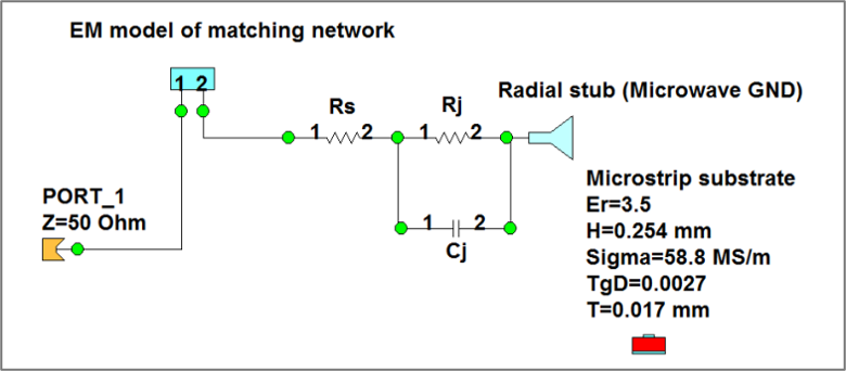
Figure 9: Final WIPL-D Microwave schematic of the matched power detector including all the elements significant at microwave frequencies
The design of a power detector can be easily accomplished if the right set of tools is available. WIPL-D Microwave is a one stop design environment providing a microwave circuit designer with several modeling options. The modeling using analytical elements can be smoothly expanded to EM analysis as an automated transfer of any schematic comprising elements with adequate layout representation to a 3D EM component is available whenever more accurate modeling is required.
A choice between non-matched or matched power detectors is driven by the context of a particular application. For the case of a matched detector, the simplest matching network topology is preferred where detector sensitivity is a must. However, the return loss values obtained by a simple network may not be sufficient for some applications. If this is the case, a more complex matching network must be designed trading-off the sensitivity for favorable return loss values. To accurately account for all the effects occurring within the matching network, use of electromagnetic modeling is highly recommended.
What is a zero-bias Schottky diode detector? A zero-bias diode does not require any external bias to operate as a detector, so it can be placed directly on the 50 Ω transmission line with adequate paths for DC and RF currents.
What is a zero-bias Schottky diode power detector used for? It is frequently used in transmitters to monitor the power coming out of a power amplifier, and in a loop with a variable attenuator and control logic it can adjust the amplifier power to a required level. At the receiver side it is used in channelized receivers and in six-port receivers.
When is a non-matched power detector adequate? When the detector is preceded by a directional coupler with a typical coupling coefficient of −20 dB or less, as in a transmitter power control loop. The loose coupling means the poor match of the detector does not affect the amplifier or the transmitter chain.
When do I need a matched power detector? When the detector is used after a filter or connected at the ports of a six-port receiver, because these circuits are very sensitive to the impedance presented at their terminals.
Why use EM modeling for the matching network? The analytical model of a T-junction that connects lines of considerably different widths, such as the 69 Ω and 20 Ω lines in this example, is not accurate. WIPL-D Microwave translates the analytical elements into an EM component automatically, so the whole matching network can be modeled accurately.
Section: Microwave Circuits
Related application notes: All application notes
Download the full application note MW_014 (PDF)