Designing a Band Pass Filter with WIPL-D Filter Designer
25-Oct-2022 Belgrade, Serbia

25-Oct-2022 Belgrade, Serbia
A process of microstrip filter design has been described in this application note with a special focus on a technique of filter optimization, a simplified case of Space Mapping method. As a result of the design process a microstrip filter ready for sample fabrication is available with minimum human and numerical effort.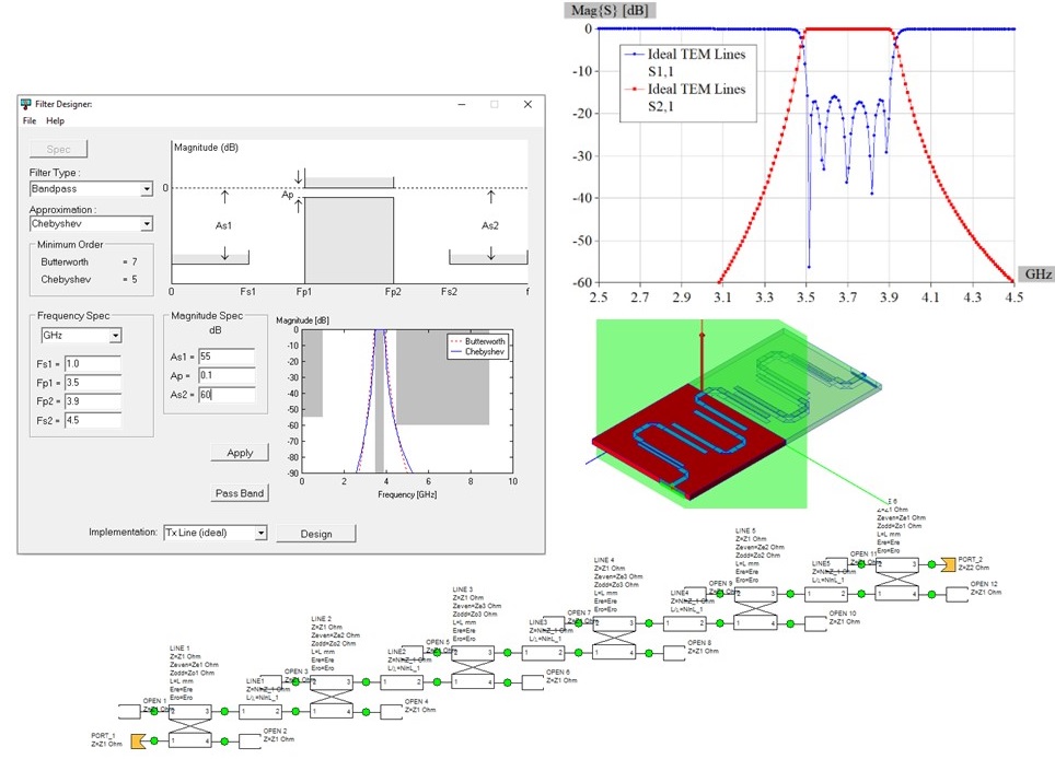
The success of the design should be high as the limitations of a standard fabrication process are taken into account during the design. This includes the choice of the best suited substrate and the dimensional constrains.
There was no need to use any special piece of computer hardware as all of the simulations required were performed with high numerical efficiency on a standard desktop machine.
Section: Microwave Circuits
For full version of the document, please check the following pdf.